NANOSCALE DEVICES (MNDL) LAB
The Marquette Nanoscale Devices Laboratory (MNDL), directed by Dr. Chung Hoon Lee, Associate Professor, Electrical and Computer Engineering (EECE), focuses on research of micro/nano scale devices. The goal of MNDL is the design, fabrication, characterization, and application of innovative micro/nanoscale sensors and actuators.
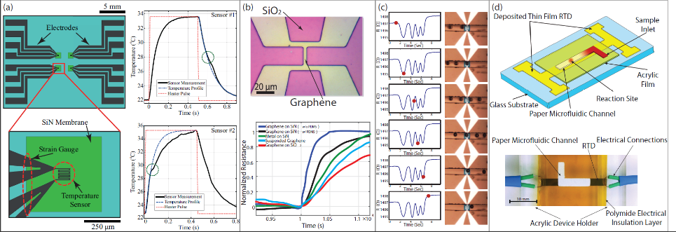
Device fabrication and characterization capabilities and activities include 1) Nano-DSC (design, development and characterization of micromachined differential scanning calorimeter for bio/chemical molecules in applications of temperature reference, rapid DNA detection, drug discovery, and bio/chemical sensors); 2) SiNWs (wafer-scale integration of silicon and silicon germanium nanowires, electrical and thermal analysis; 3) Tip-based nanofabrication (developing micromachined bow tie antenna for local optical field enhancements to controlled nanowire array growth; 4) Molecular electronics (design and fabrication of multi-nanogap electrodes as a platform for single molecule electronics, electrical and thermal measurement of single molecule and analysis); and 5) AFM/SPM probes (multi-functional AFM/SPM probe development and characterization).
Dr. Lee’s group also uses the Wisconsin Center for Microelectronics (WCAM) fabrication facility as well as the University of Wisconsin (Milwaukee) High resolution Scanning Electron Microscope (SEM) and Transmission Electron Microscope (TEM) facility.
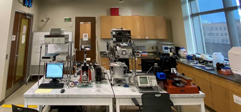
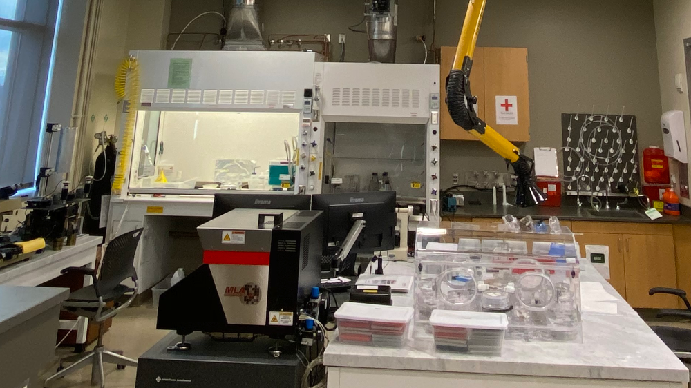
The fabrication equipment in MNDL includes: Heidelberg Mask less Aligner MLA100 system; Horiba Raman Spectroscopy; NT-MDT Atomic Force Microscopy (AFM) Solver NANOAFM system; 40GHz E8363B Agilent vector network analyzer; Atomic Layer Deposition (ALD); High temperature oxidation furnace for thermal SiO2 growth; Key High 2KVA high vacuum dual source thermal evaporator; MILA-5000 Mini Lamp Annealer; Reactive Ion Etcher (RIE) for thin film etch such as Si, SiO2, SixNy and polymers; Optical lithography: mask aligner; HMDS vapor coating, and photoresist spinner; Metal evaporator and sputtering system; Wet chemical bench (fume hood) for base/acid and solvent; Silicon anisotropic wet etching system; Wire-bonder; Anodic bonding system for glass/silicon bonding; Scanning Electron Microscope (SEM and Chemical Vapor Deposition (CVD) system for nanowire growth.
The characterization equipment include the following electrical measurement system with Labview control: Signatone probe station with digital image capture; HP4145 Semiconductor analyzer; HP 4140B Picoammeter / DC Voltage Source; AGILENT-HP 3312A Function Generator; Keithley 2400 SourceMeter; Keithley 2600 two channel SourceMeter; Agilent vector network analyzer; SR830 — 100 kHz DSP lock-in amplifier; SR844 High Frequency Lock-In Amplifier, 25 kHz to 200 MHz; SR560 Current Preamplifier; SR560 Voltage Preamplifier; 2MHz laser strobe system; Home-made vacuum chamber for ultrahigh precision current/voltage measurement.
MNDL Lab Location
Engineering Hall 277
1637 W. Wisconsin Avenue
Milwaukee, WI 53233
Contact:
Dr. Chung Hoon Lee
Associate Professor of Electrical and Computer Engineering
(414) 288-4460
email